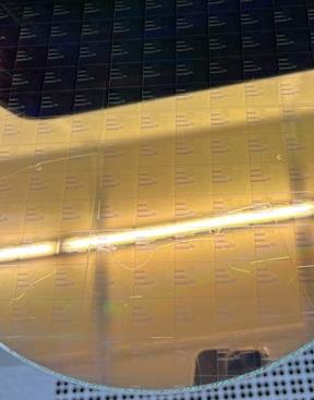
A color splitter built from a vertical waveguide is the foundation of eyeo’s NCOS® technology. The original research was published by imec, Ghent University, and KU Leuven at the 2023 IEEE International Electron Devices Meeting (IEDM) in San Francisco.
This is the initial paper that started it all. Building on the foundation established and proven at imec, eyeo now holds 26 patents and is investing in the full in-house engineering capability required to deliver sensors to customers at volume scale.
The original paper is available to download in full below.
CMOS image sensor pixel sizes have reached 0.56 micron, well below the Abbe diffraction limit. High-end cameras still favor larger pixels, because very small pixels capture a limited signal, resulting in lower signal-to-noise ratio.
Bayer color filters absorb a substantial share of incoming light, reducing signal-to-noise ratio. They limit the image quality the sensor can actually deliver. And because they rely on chemically engineered absorption, the combinations of absorption characteristics and high-resolution patterning that are achievable stay limited.
There have been attempts in the past to solve this problem using nanophotonic structures but based on diffraction principles. These methods addressed the light-absorption problem of color filters, but did not improve image resolution beyond the Abbe limit. The Abbe limit is itself a diffraction phenomenon, so any method that also relies on diffraction cannot move beyond it.
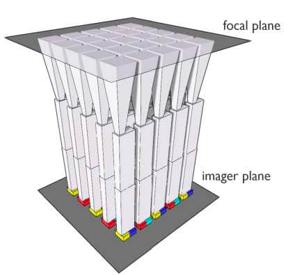
eyeo’s sensors, featuring NCOS® technology, split color using the beating pattern between a symmetric and an antisymmetric mode inside a multimode vertical waveguide. The higher refractive index of the Si₃N₄ waveguide material compresses the effective photon wavelength relative to air, enabling the color splitter to separate colors at pixel sizes below the diffraction limit.
Each vertical waveguide color splitter has a rectangular cross-section, topped by a tapered entrance funnel positioned at the focal plane of the camera lens. Incident white light is squeezed into a smaller size as it passes through the taper. The taper feeds that light asymmetrically into the straight rectangular waveguide section below, which excites both a symmetric and an antisymmetric propagation mode. Each wavelength of light propagates at a different relative speed between the two modes, so the waveguide’s dimensions can be tuned to set a desired color composition at its left and right exits.
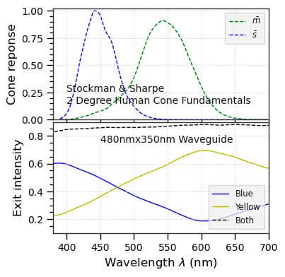
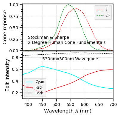
A single vertical waveguide color splitter divides the spectrum into two parts, exiting left or right, at a crossing wavelength set by its geometry. Matching full human color vision, which relies on three cone types, requires combining two waveguide designs together: one with a crossing point between blue and green, around 480 nanometers, and one with a crossing point between green and red, around 580 nanometers. Each design contributes a left and a right signal, for four signals total that reconstruct full color information.
The color splitter stack uses silicon nitride waveguides embedded in a silicon dioxide matrix, a standard CMOS-compatible material system, processed on 300mm wafers. The 6-micron-tall waveguides were built as three repeated 2-micron layers, each involving SiCN / SiO2 deposition, trench patterning in SiO2, trench filling with conformal deposition of SiN, planarization.
The structure was first processed on a blank silicon wafer. For optical characterization, it was bonded to a glass carrier and the silicon substrate was removed by grinding and etching, since silicon is opaque in the visible range.
TiN reflective layers were added at both the top and bottom of the waveguide stack, the top layer covering unused space between input tapers, and the bottom layer selectively blocking one side of individual waveguide exits, which let researchers directly visualize which color was exiting each side.
Two separate vertical waveguide designs were used to demonstrate different aspects of the technology.
Under white-light illumination, a color splitter design measuring 620 by 250 nanometers, tuned to split blue light from the rest of the spectrum, showed blue light exiting its left side and yellow light exiting its right side, confirmed by RGB camera imaging at 100x magnification. Separately, sweeping waveguide long-axis and short-axis dimensions across a broader design space (480–650nm by 200–350nm) showed the color transition point could be shifted continuously from a blue-green crossing to a green-red crossing.
A separate 560 by 300 nanometer design was tested with confocal microscopy, illuminated individually with blue (450nm), green (532nm), and red (632nm) lasers and imaged with a high-numerical-aperture (0.95) objective. Blue light concentrated dominantly at the right exit, red light concentrated dominantly at the left exit, and green light split close to evenly between both exits, closely approximating human cone sensitivity.
The team benchmarked their two-waveguide color splitter design against a public database of Bayer filters from high-end full-frame commercial cameras, using the Vora metric for color-filter quality. To avoid tuning the result to a single reference viewer, they extended the assessment beyond the standard CIE 1931 observer to a broad demographic set of human color observers spanning races, continents, and ages.
The assessment used three different detector options underneath the optical stack: two commercial CIS detectors and an alternative CMOS-compatible thin-film photodetector, a 275-nanometer-thick CsPbI2Br perovskite detector built in-house, each paired with a commercial UV filter.
The color splitter reached a Vora value above 95 percent, placing it on par with most high-end commercial cameras, while the combined light output at both exits of each waveguide design exceeded 90 percent across the 400 to 700 nanometer visible range, a throughput level the paper states surpasses color filters.
eyeo’s sensors, featuring NCOS® technology, build on this mode-beating, filter-free, sub-diffraction color splitting principle, now being developed for commercial image sensors across smart city applications, industrial inspection, XR headsets and smart glasses, physical AI and mobile phones.
The full technical paper, including the fabrication stack details and complete Vora value comparison, is available to download below.
S. Kang, M. Benelajla, R. Mac Ciarnain, F. Ali, A. Papadopoulou, O. Shramkova, L. Witters, J. De Vos, P.E. Malinowski, P. Heremans, N. Le Thomas, B. Figeys, R. Gehlhaar and J. Genoe “Wafer-level-integrated vertical-waveguide sub-diffraction-limited color splitters.” Imec, Ghent University, KU Leuven. Funded by FWO Project S004322N (GigaPixel).